How Is Reinforcement Learning Transforming Modern Silicon Architecture?
The semiconductor industry is undergoing a drastic change as traditional tools of Electronic Design Automation (EDA) are not able to keep up with the increased complexity of modern chips. Hundreds of millions or even billions of transistors are packed into a single microchip. Designing such a chip used to require months of human labor in the form of countless manual changes to the layout, physical floorplanning and signal routing. However, deep learning has recently transformed the process of optimizing physical layout into a high-dimensional game that can be played by autonomous agents. These agents can be trained to fulfill a variety of tasks, including architecture-specific constraints, and in the end enable the hardware engineer to reach the optimal trade-off between Power, Performance, and Area (PPA) in a fraction of the time that would be required by human engineers.
By mastering the intersection of hardware description languages and the latest AI frameworks, engineers can become very valuable for top technology companies globally. You can learn all this in a comprehensive reinforcement learning chip design course in Mumbai and apply your newly found knowledge to become a bridge between fundamental EDA skills and the latest automation tools.
There are key shifts happening in the way semiconductor design is operated using reinforcement learning:
- Faster Floorplanning Cycles: RL-based agents are able to explore millions of different designs in a few hours, whereas a human would take months to come up with nearly as many designs.
- Automated Congestion and Thermal Reduction: Use of deep learning neural networks to automatically manage component density to avoid parasitic capacitance and thermal “hot-spots” on the silicon substrate.
- Optimal Placement & Routing (P&R): This technology uses specialized reinforcement learning algorithms that evaluate and optimize all design rule checks to create the most optimal layout possible automatically, with no human intervention.
- Intelligent Testbench Generation: Deep learning models automatically generate testbatches for verification of functionality of design to detect edge-case bugs and to ensure that design functions as expected before actual tape-out and fabrication.
- Reduced Development Costs: Automating design verification and tape-out can lead to cost savings for designs that go into production quickly and have fewer errors as they enter service.
Why Is Deep Reinforcement Learning Becoming Essential for Placement & Routing?
Macro block placement and signal routing are typically the two most time-consuming steps in VLSI physical design. As chips are shrinking down to sub-3nm nodes, the number of possible placements for the macro blocks can run into millions. All of these possible placements can be explored by human designers or by rule-based design tools, but it is unlikely that the global optimum will be found. Deep reinforcement learning can solve this problem by modeling chip floorplanning as an environment in which a designer can learn to map floorplans to rewards using an agent that is trained in deep reinforcement learning for chip design in Mumbai.
The engineers who undergo in-depth training in chip placement with deep reinforcement learning in classes in Mumbai learn to create end-to-end automated physical design tools using state-of-the-art open-source as well as commercial design tools.
Some key advantages of deep RL for placement and routing:
- Continuous Reward Optimization: Custom reward functions can now optimize wire length, signal delay and even routing congestion simultaneously as the design space is searched.
- Handling High-Dimensional State Space: Deep learning architectures are used to handle the large amount of continuous spatial information for the high-dimensional state space of VLSI chip floorplanning.
- Design Rule Checking (DRC) Compliance: Deep RL agents are trained to always follow design rules of physical manufacturing, thus greatly reducing the time spent on cleaning up the designed layout after placement.
- Cross-Process Nodes Scalability: With sufficient fine-tuning, the same deep reinforcement learning model can be applied across various technology nodes.
- Reducing Design Iterations: Removing the need for designers to manually go through iterations of trial and error for routing, enabling them to concentrate on higher-level system architecture.
What are the key modules and key skill sets that are taught in an industry-relevant curriculum?
The ever-changing domain of AI-driven hardware design requires a unique combination of established VLSI fundamentals and modern machine learning techniques along with their practical implementation using industry-standard EDA tools. A course in hardware design using AI can start with basic hardware description languages like Verilog and SystemVerilog, followed by the advanced topics of reinforcement learning, including PyTorch and TensorFlow, and their application to the mapping of floorplanning problems to Markov Decision Processes (MDP), the definition of dynamic reward functions, and the implementation of deep Q-learning and policy gradient methods. Offered as structured classes in reinforcement learning chip design in Mumbai, these courses will help hardware designers learn to develop scalable automation scripts for their work and work under the guidance of industry experts.
These skill sets, learned by the students, will help them in optimizing silicon for real-world problems like timing closure, congestion, thermal, etc. This kind of training in the field of reinforcement learning for chip design will make engineers employable in the best R&D organizations in the world.
Essential skill modules for the curriculum to make students employment-ready to join R&D functions in leading global semiconductor companies include:
- Fundamentals of Hardware Automation: Learn the basic skills of a hardware automation engineer to write a Verilog design, do RTL synthesis and set up a floorplanning environment using Cadence and Synopsys scripts for automation.
- Machine Learning & RL Foundations: Study of fundamental concepts in machine learning & RL, such as Q-learning, PPO, and DDPG, and how to apply them to spatial problems like floorplanning and routing.
- Custom Environment Development: Students will learn to create and customize environments to solve the physical chip placement and signal routing problems in order to create a challenging and realistic scenario for RL to solve within the framework of OpenAI Gym environments.
- Automated Verification & PPA Optimization: Implement and integrate AI to predict timing violations and parasitic capacitance and to optimize PPA (power-performance-area) of designed chip components.
- Capstones & Production Integration: Hands-on experience in designing custom chip components using tools that are integrated with automated physical placement algorithms designed specifically to adhere to design rules.
What Career Opportunities and Salary Trends Exist in AI-Driven Hardware Design?
With an unprecedented demand of engineers that can embed artificial intelligence into silicon design, semiconductor companies that design next-generation AI accelerators, autonomous vehicles, and high-performance computing systems are competing for engineers that can design hardware at scale and write automated designs in a variety of languages. As silicon gets to be too slow to scale, design optimization of layout becomes a major performance improvement area. We will train our students to design a chip from scratch and use deep reinforcement learning to get the best possible performance out of the chip in Mumbai to create top hardware design engineers with exposure to the best in class software technologies to place them in the highest-paying jobs in the hardware design domain.
In the last few years, as major semiconductor MNCs expanded their R&D centers in India, the compensation for a specialized chip design engineer has been higher than that of a software engineer. Leading product companies like Google, Facebook, Amazon, etc., pay very competitive starting salaries to design engineers at the entry level and much more to experienced RL hardware architects.
Some Key Career Pathways & Financial Growth (salary) Trends in this field:
- AI Hardware Architect: Design Novel Neural Network Accelerators and Optimize Compute Engines for Emerging Generative AI Models.
- Physical Design & EDA Engineer: Write automated placement and routing tools to speed up design othe designf modern chips.
- VLSI Machine Learning Specialist: Apply deep learning to predict post-layout parasitics, thermal hotspots, timing constraints, etc., before the actual tape-out.
- Salary growth: Very competitive salaries for fresh graduates in specialized fields with very rapid growth in salary for senior technical people.
- Global Career Mobility: Be ready to get hired by the best tech companies in the US, Europe and Asia, which have large research and development centers having automated silicon design engineers to work on cutting-edge designs.
How Does Hands-On Training Bridge the Gap Between Theory and Industry Placement?
While theoretical knowledge of the latest reinforcement learning algorithms helps to tackle challenging physical design problems on real silicon, in the industrial semiconductor world dealing with noisy data, complex constraints and tight timing margins is the norm. To connect abstract mathematical designs (reward functions) to physical design space (cell density, net length, interconnect delays, …) to create practical chips, hands-on experience with a large number of projects in practical chip placement using deep reinforcement learning training in Mumbai is essential. While theoretical knowledge of the latest reinforcement learning algorithms helps to tackle challenging physical design problems on real silicon, in the industrial semiconductor world dealing with noisy data, complex constraints and tight timing margins is the norm.
Interactive studio environment along with projects and guidance to debug real-world placement problems as opposed to learning about solving toy problems in class. Practical training enables the student to become effective immediately in high-impact engineering projects.
- Core components of a practical learning approach include:
- Hands-on Practice with EDA Tools: Industry-specific automation tools and open-source design tools for layout synthesis.
- Live Layout Optimization Projects: Create end-to-end reinforcement learning models that can be used for optimization of open-source floorplans for microchips.
- DRC Violations Troubleshooting: Identify, diagnose and fix design rules Violations encountered during automated layout runs.
- Portfolio & Code Repository Development: Create a project for placement of a floor plan of an open-source microchip and create a documented GitHub repository to demonstrate how one can create custom RL environments and implement silicon placement using reinforcement learning for recruiters.
- Mock Interviews & Resume Scaffolding: Practice your digital design, computer architecture, and reinforcement learning skills with mock interviews. Create a robust resume with the help of scaffolding.
How Do Integrated Technology Stacks Complement Hardware AI Automation?
The semiconductor design and physical layout automation software exists within a massive ecosystem of enterprise IT, cloud computing, and software application stacks. The software used to track the design’s complementary tasks interacts with the designer building the machine learning hardware. In mastering these software tracks that interact with the designer building machine learning hardware in semiconductor design, the engineer builds full-stack industrial software applications that interact with smart silicon hardware.
The following are top technologies that can complement advanced AI chip design:
Got Questions? Here Are Some FAQs
1. Who is eligible to enroll in these AI-driven chip design programs?
Who can enroll in this course? VLSI designers, fresh electronics graduates, software professionals, data analysts/scientists, and other AI/ML enthusiasts interested in learning customized hardware for ML/AI and also learning to program smart chips.
2. Is prior experience in machine learning required before starting?
The course begins with the basic concepts of machine learning and reinforcement learning before proceeding to learn the concepts of custom hardware environments and automated floorplanning models using EDA tools such as OpenROAD for physical design scripting.
3. What software toolsets and libraries will I work with during training?
The training uses Python and various tools and libraries including PyTorch/TensorFlow and OpenAI Gym/Gymnasium (to train RL agents) and open-source EDA tools (OpenROAD) and industrial physical design scripting tools (for placing and routing chips).
4. How does reinforcement learning differ from traditional EDA heuristics in physical placement?
As compared to traditional EDA heuristics that are typically encoded as a fixed program, Reinforcement Learning agents learn by interacting with their environment and learn the optimal placement strategy for a given chip as they go along, eventually achieving better PPA for a given design, often faster.
5. Does SevenMentor provide job placement support after course completion?
Yes, SevenMentor provides placement assistance after course completion. The assistance includes portfolio building, mock interviews, resume building, and placement through referral to corporate clients of SevenMentor.
Related Links:
Anthropic AI Tool
What is Writesonic
Career Objectives For Fresher
Resume Tips For Software Developers
Do visit our channel to know more: SevenMentor
 Look Forward To Building A Future-Ready Career In Machine Learning
 Gain In-Depth Knowledge Of Algorithms, Predictive Modeling, And Machine Learning Implementation
 Kickstart Your Machine Learning Career Today At The Top Choice For Enthusiasts
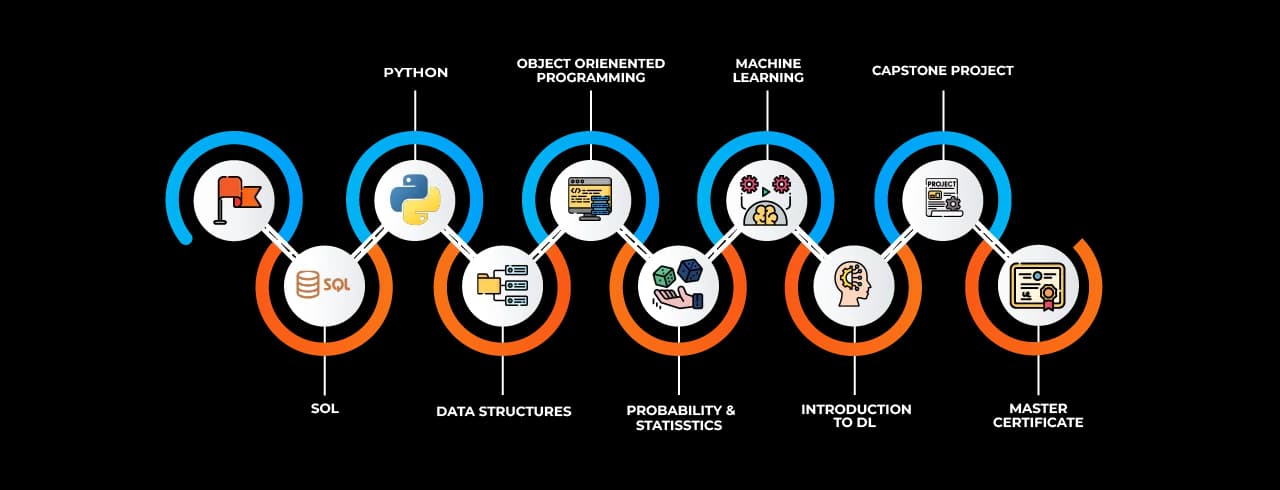
 Scikit learnA machine learning library for predictive modeling and analysis.
 Probability & Statistics Fundamental concepts for making data-driven predictions and decisions.
 Machine Learning Algorithms Core algorithms that enable machines to learn patterns from data
 Feature EngineeringTechniques to transform raw data into meaningful input for models.
 Data PreprocessingCleaning and preparing data to improve model performance.
 Model Evaluation & ValidationMethods to assess and fine-tune machine learning models.
 Hyperparameter TuningOptimizing model parameters to enhance accuracy and efficiency.
 PythonA versatile programming language widely used for machine learning.
R: A statistical computing language popular for data analysis and visualization.
Scikit-learn: A powerful Python library for implementing machine learning algorithms.
PythonA versatile programming language widely used for machine learning.
R: A statistical computing language popular for data analysis and visualization.
Scikit-learn: A powerful Python library for implementing machine learning algorithms.
 Jupyter NotebookAn interactive environment for coding, visualizing, and documenting ML projects